Microfab Lab provides a broad range of fabrication and characterization technologies to support research and development in micro- and nanosystems. Our capabilities include semiconductor processes, advanced polymer-based structuring, development of biocompatible devices, and high-precision micromachining, supported by experienced engineers and embedded within the multidisciplinary research environment of Eindhoven University of Technology (TU/e), enabling integrated support across the design and fabrication workflow.
Advanced tools for micro- and nanofabrication

Laser Micromachining
Glass microdevice fabrication with sub-micron precision
Microfab Lab hosts the FEMTOprint platform, a femtosecond laser micromachining system capable of direct writing inside transparent materials such as fused silica. This technology enables the creation of true 3D microstructures without masks or complex alignment procedures.
Key applications include:
- Microchannels and cavities for lab-on-glass devices
- Optical waveguides, microlenses, and photonic elements
- Integrated fluidic ports, mixers, and nozzles
- Micromechanical components, including flexures and resonators
Post-processing with chemical etching allows internal features to be selectively revealed, resulting in monolithic, high-precision glass microdevices—ideal for life science, photonics, and micro-optics applications.

Polymer & 3D Fabrication
Flexible platforms for soft materials and complex geometries
Beyond traditional MEMS processing, we offer dedicated tools for the fabrication of structures in polymers and soft materials, ideal for biomedical, microfluidic, and flexible electronics applications.
Highlights include:
- SU-8 and PDMS microfabrication for lab-on-chip and soft sensor systems
- Soft lithography, micro-molding, and replica casting
- Micropatterned hydrogel scaffolds for tissue engineering and cell culture
- A range of 3D printers, from stereolithography (SLA) to fused deposition modeling (FDM) for realizing complex 3-dimensional polymer devices.
These platforms enable rapid prototyping of functional structures and are well suited for integrating fluidic, optical, or mechanical functions into bio-compatible systems.

Modeling & Simulation
Supporting design, verification, and optimization
We provide a wide range of computational and physical analysis tools. This supports everything from early-stage modeling to device verification.
Available services include:
- Microfluidics simulations using advanced computational modeling
- MEMS and mechanical FEM simulations
- Optical modeling for integrated photonic and micro-optic systems
- Electrical testing of microdevices, including impedance and capacitance measurement
- Surface and material analysis (profilometry AFM, contact angle, interferometry)
These capabilities enable iterative design and rapid feedback, shortening development cycles and increasing design confidence.

ML2 Biolab
From microfabrication to biological application
To support life science research and biomedical prototyping, Microfab Lab offers a dedicated bio-lab environment designed for interfacing microdevices with biological samples.
Capabilities include:
- Cell culture workstations for live cell handling
- Spheroid and organoid platform development
- Microfluidic interfacing setups for flow control and perfusion
- Live-cell Microscopy and imaging stations for device-biology interaction studies
- A ML-certified biolab
- Organ-on-Chip / Microphysiological Systems development and characterization
This setup enables seamless testing of organ-on-chip systems, lab-on-chip diagnostics, and biosensing platforms, directly within a bio-compatible environment.
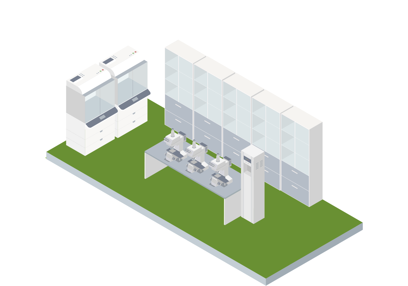

Cleanroom Processing
Operating at ISO Class 7 level for standard and custom flows
Our cleanroom is the core of the Microfab Lab, enabling a full range of front-end microfabrication processes. We support both standard microtechnology and tailor-made workflows, accommodating a variety of materials and device architectures.
Capabilities include:
- Photolithography: Mask aligners and projection lithography systems for feature sizes down to sub-micron scale.
- Wet Etching: Buffered HF, KOH, and other etchants for anisotropic and isotropic processing.
- Thin-Film Deposition: Physical Vapor Deposition (PVD) – Sputtering for metals and dielectrics.
- Surface Modification: Plasma and UV-Ozone treatment.
- Direct access to TU/e Nanolab for advanced micro- and nanofabrication technologies.
We support substrates ranging from silicon and glass to polymers and compound materials, and routinely process 4-inch wafers.